
Jan 10 2025
New Material for Nanoconductors
 One of the things I have come to understand from following technology news for decades is that perhaps the most important breakthroughs, and often the least appreciated, are those in material science. We can get better at engineering and making stuff out of the materials we have, but new materials with superior properties change the game. They make new stuff possible and feasible. There are many futuristic technologies that are simply not possible, just waiting on the back burning for enough breakthroughs in material science to make them feasible. Recently, for example, I wrote about fusion reactors. Is the addition of high temperature superconducting material sufficient to get us over the finish line of commercial fusion, or are more material breakthroughs required?
One area where material properties are becoming a limiting factor is electronics, and specifically computer technology. As we make smaller and smaller computer chips, we are running into the limits of materials like copper to efficiently conduct electrons. Further advance is therefore not just about better technology, but better materials. Also, the potential gain is not just about making computers smaller. It is also about making them more energy efficient by reducing losses to heat when processors work. Efficiency is arguably now a more important factor, as we are straining our energy grids with new data centers to run all those AI and cryptocurrency programs.
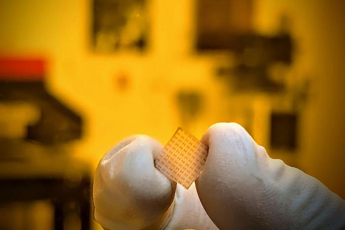
This is why a new study detailing a new nanoconducting material is actually more exciting than it might at first sound. Here is the editor’s summary:
Noncrystalline semimetal niobium phosphide has greater surface conductance as nanometer-scale films than the bulk material and could enable applications in nanoscale electronics. Khan et al. grew noncrystalline thin films of niobium phosphide—a material that is a topological semimetal as a crystalline material—as nanocrystals in an amorphous matrix. For films with 1.5-nanometer thickness, this material was more than twice as conductive as copper. —Phil Szuromi
Greater conductance at nanoscale means we can make smaller transistors. The study also claims that this material has lower resistance, which means more efficient – less waste heat. They also claim that manufacturing is similar to existing transistors at similar temperatures, so it’s feasible to mass produce (at least it seems like it should be). But what about niobium? Another lesson I have learned from examining technology news is to look for weaknesses in any new technology, including the necessary raw material. I see lots of battery and electronic news, for example, that uses platinum, which means it’s not going to be economical.
Niobium is considered a rare metal, and is therefore relatively expensive, about $45 per kilogram. (By comparison copper goes for $9.45 per kg.) Most of the world’s niobium is sourced in Brazil (so at least it’s not a hostile or unstable country). It is not considered a “precious” metal like gold or platinum, so that is a plus. About 90% of niobium is currently used as a steel alloy, to make steel stronger and tougher. If we start producing advanced computer chips using niobium what would that do to world demand? How will that affect the price of niobium? By definition we are talking about tiny amounts of niobium per chip, the wires are only a few molecules thick, but the world produces a lot of computer chips.
How all this will sort out is unclear, and the researchers don’t get into that kind of analysis. They basically are concerned with the material science and proving their concept works. This is often where the disconnect is between exciting-sounding technology news and ultimate real-world applications. Much of the stuff we read about never comes to fruition, because it simply cannot work at scale or is too expensive. Some breakthroughs do work, but we don’t see the results in the marketplace for 10-20 years, because that is how long it took to go from the lab to the factory. I have been doing this long enough now that I am seeing the results of lab breakthroughs I first reported on 20 years ago.
Even if a specific demonstration is not translatable into mass production, however, material scientists still learn from it. Each new discovery increases our knowledge of how materials work and how to engineer their properties. So even when the specific breakthrough may not translate, it may lead to other spin-offs which do. This is why such a proof-of-concept is exciting – it shows us what is possible and potential pathways to get there. Even if that specific material may not ultimately be practical, it still is a stepping stone to getting there.
What this means is that I have learned to be patient, to ignore the hype, but not dismiss science entirely. Everything is incremental. It all adds up and slowly churns out small advances that compound over time. Don’t worry about each individual breakthrough – track the overall progress over time. From 2000 to today, lithium-ion batteries have about tripled their energy capacity, for example, while solar panels have doubled their energy production efficiency. This was due to no one breakthrough, just the cumulative effects of hundreds of experiments. I still like to read about individual studies, but it’s important to put them into context.