
Feb 07 2023
2D Computer Chips
 Communicating about emerging technology can be challenging because it is often difficult to find the real obstacles to the widespread adoption of that technology. Most reporting focuses on the hype. Technical articles are the most helpful, but they are usually not geared to a non-expert audience. This means that they don’t always give a big-picture view from a practical perspective. Rather, they are focusing on the technical details relevant to the specific study. Usually I learn about a major hurdle from an article which purports to solve it – although even then they may be focused on the problems they can potentially solve while not explicitly discussing remaining hurdles. It takes time and digging to piece together a full picture. Sometimes I have the opportunity to speak with the right kind of expert, or they themselves engage in helpful science communication and spell it out.
One of the many examples of this is 2D material – material that is one atom or molecule thick. The most famous such material is graphene, a single atom thick sheet of carbon arranged in a “chicken wire” pattern. It’s easy to find articles discussing all the amazing physical properties of graphene and other 2D materials and all the potential future applications. This may leave one curious as to why we have not been seeing more applications using this material. The short answer is that we do not yet know how to mass produce graphene in bulk and without defects. We can crank out lots of small pieces (or short pieces of carbon nanotubes, which are essentially rolled-up graphene), but they are both short and riddles with defects. This doesn’t matter if we are just adding it to as filler to another material to make it stronger, but won’t work for most of the exciting applications. Small defects also matter because one such defect can be a vulnerable point from which the entire sheet or nanotube and unzip.
Another application with amazing potential but with serious hurdles in the way is 2D computer chips. Silicon-based chips have proven to be a powerful technology, that has kept Moore’s law (the general observation that the density of transistors on a chip has roughly doubled every 18 months or so) going for decades. But silicon-based chips are running into some fundamental limits with the laws of physics. You can only make transistors so small before they cannot function. Transistors are now down to the 2 nm size, and this is close to the limit where classical physics transitions to quantum physics (to be clear, we are not talking about quantum computers, which is an entirely different technology). The limitation is the ability to control the flow of electrons through transistors. If the flow becomes chaotic or uncontrollable, then the chip doesn’t work. (This is an admittedly simplified non-technical description of the issue.)
This is why chip makers are looking for a new technology to shift over to that doesn’t have the same limit as current silicon chips, and that is where 2D materials come in. At one atom thick they are as small as you can get. They also have great conducting properties, and can be “doped” (with the addition of other elements) to tweak those properties to make them semiconductors if necessary. So why aren’t our desktop computers already using graphene or some other 2D material-based chips? We are still stuck with the two basic problems – mass producing defect-free 2D materials. These are non-trivial problems that engineers have been working on for almost two decades (since graphene was developed in 2004).
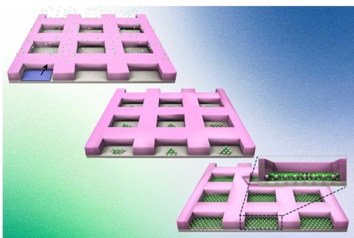
A recent study from researchers at MIT proposes a method for solving the defect-free problem – Non-epitaxial single-crystal 2D material growth by geometric confinement. “Epitaxial” refers to the phenomenon when one crystal layer grows on top of another, and its orientation is determined by the existing layer. So non-epitaxial would me that the crystal layer orientation is not determined by the crystal seed. The key technology here is the “geometric confinement”, which is a way of controlling the growth of this 2D crystal layer so that it has the desired shape without defects. As I noted above, in the article the authors spell out the specific technical limits to making 2D chips:
Nevertheless, 2D-based electronics have not been commercialized, owing mainly to three critical challenges: i) precise kinetic control of layer-by-layer 2D material growth, ii) maintaining a single domain during the growth, and iii) wafer-scale controllability of layer numbers and crystallinity.
These three features refer to the ultimate configuration of the 2D crystal. They further explain:
Here we introduce a deterministic, confined-growth technique that can tackle these three issues simultaneously, thus obtaining wafer-scale single-domain 2D monolayer arrays and their heterostructures on arbitrary substrates.
Essentially they are able to control the growth and shape of the crystal, which can be in any configuration they choose. The basic technique is to use vapor deposition to deposit material across a silicon wafer that acts like a template. The crystal seeds that get deposited would normally grow in random orientations and sizes, but they control the crystal growth by depositing silicon dioxide on the wafer to form little pockets in the desired orientation. These pockets control where the crystal seeds land and how big they grow – constraining them to form only a single layer crystal.
The result, the researchers claim, is a defect-free 2D crystal semiconductor of any design they wish. So have they done it? Have they created a 2D semiconductor chip that can replace silicon? Study author Jeehwan Kim says:
“Until now, there has been no way of making 2D materials in single-crystalline form on silicon wafers, thus the whole community has almost given up on pursuing 2D materials for next-generation processors. Now we have completely solved this problem, with a way to make devices smaller than a few nanometers. This will change the paradigm of Moore’s Law.”
I suppose we will see. What I did not see discussed was how easily this process can be scaled to industrial levels. Unless you can mass produce billions of such chips in a cost effective manner, the technology may be interesting but won’t transform the industry. Of course I hope this works as advertised. This still means it will be at least a few years to develop the industrial process, and this may not be the exact final method that gets used. But research like this does increase hope that we do have 2D semiconductors in our future.