
Jan 25 2024
DNA Directed Assembly of Nanomaterials
 Arguably the type of advance that has the greatest impact on technology is material science. Technology can advance by doing more with the materials we have, but new materials can change the game entirely. It is no coincidence that we mark different technological ages by the dominant material used, such as the bronze age and iron age. But how do we invent new materials?
Historically new materials were mostly discovered, not invented. Or we discovered techniques that allowed us to use new materials. Metallurgy, for example, was largely about creating a fire hot enough to smelt different metals. Sometimes we literally discovered new elements, like aluminum or tungsten, with desirable properties. We also figured out how to make alloys, combining different elements to create a new material with unique or improved properties. Adding tin to copper made a much stronger and more durable metal, bronze. While the hunt for new usable elements is basically over, there are so many possible combinations that researching new alloys is still a viable way to find new materials. In fact a recent class of materials known as “superalloys” have incredible properties, such as extreme heat resistance.
If there are no new elements (other than really big and therefore unstable artificial elements), and we already have a mature science of making alloys, what’s next? There are also chemically based materials, such as polymers, resins, and composites, that can have excellent properties, including the ability to be manufactured easily. Plastics clearly had a dramatic effect on our technology, and some of the strongest and lightest materials we have are carbon composites. But again it feels like we have already picked the low-hanging fruit here. We still need new better materials.
It seems like the new frontier of material science is nanostructured material. Now it’s not only about the elements that a material is made from, it is how the atoms of that material are arranged on a nano-scale. We are just at the beginning of this technology. This approach has yielded what we call metamaterials – substances with properties determined by their structure, not just their composition. Some metamaterials can accomplish feats previously thought theoretically impossible, like focusing light beyond the diffraction limit. Another class of structured material is two-dimensional material, such as carbon nanofibers.
The challenge of nanostructured materials, however, is manufacturing them with high quality and high output. It’s one thing to use a precise technique in the lab as a proof of concept, but unless we can mass produce such material they will benefit only the highest end users. This is still great for institutions like NASA, but we probably won’t be seeing such materials on the desktop or in the home.
This brings us to the topic of today’s post – using DNA in order to direct the assembly of nanomaterials. This is already in used, and has been for about a decade, but a recent paper highlights some advances in this technique: Three-dimensional nanoscale metal, metal oxide, and semiconductor frameworks through DNA-programmable assembly and templating.
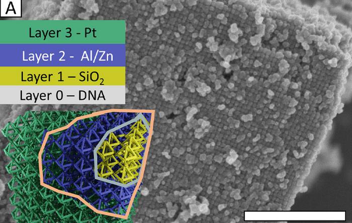
There are a few techniques being used here. DNA is a nanoscale molecule that essentially evolved to direct the assembly of proteins. The same process is not being used here, but rather the programmable structure of DNA means we can exploit it for other purposes. The first step in the process being outlined here is to use DNA in order to direct the assembly of a lattice out of inorganic material. They make the analogy that the lattice is like the frame of a house. It provides the basic structure, but then you install specific structures (like copper pipes for water and insulation) to provide specific functionality.
So they then use two different methods to infiltrate the lattice with specific materials to provide the desired properties – semiconductors, insulators, magnetic conduction, etc. One method is vapor-phase infiltration which introduces the desired elements as a gas, which can penetrate deeply into the lattice structure. The other is liquid phase infiltration, which is better at depositing substance on the surface of the lattice.
These combinations of methods address some of the challenging of DNA directly assembly. First, the process is highly programmable. This is critical for allowing the production of a variety of 3D nanostructured materials with differing properties. Second the process takes advantage of self-assembly, which is another concept critical to nanostructured materials. When you get down to the 30 nm scale, you can’t really place individual atoms or molecules in the desired locations. You need a manufacturing method that causes the molecules to automatically go where they are supposed to – to self assemble. This is what happens with infiltration of the lattice.
The researchers also hope to develop a method that can work with a variety of materials to produce a range of desirable structures in a process that can be scaled up to manufacturing levels. They demonstrate at least the first two properties here, and show the potential for mass production, but of course that has yet to be actually demonstrated. They worked with a variety of materials, including: ” zinc, aluminum, copper, molybdenum, tungsten, indium, tin, and platinum, and composites such as aluminum-doped zinc oxide, indium tin oxide, and platinum/aluminum-doped zinc oxide.”
I don’t know if we are quite there yet, but this seems like a big step toward the ultimate goal of mass producing specific 3D nanostructured inorganic materials that we can program to have a range of desirable properties. One day the computer chips in your smartphone or desktop may come off an assembly line using a process similar to the one outlined in this paper. Or this may allow for new applications that are not even possible today.